Wafer sorting plays a vital role in semiconductor production by identifying defective wafers early in the process. This helps to eliminate substandard wafers before they progress further down the production line, ensuring that only high-quality wafers are used in the final product. As wafer sizes continue to increase and the complexity of semiconductor devices grows, the need for more sophisticated sorting equipment has never been greater.
The latest wafer sorting systems provide enhanced throughput, greater flexibility, and integration with existing production lines, making them essential for meeting the demands of modern fabs.

Advanced wafer sorting systems are designed for high-speed operation, enabling manufacturers to sort large volumes of wafers without sacrificing precision. This is crucial in semiconductor fabs, where high throughput is essential to meet the demands of mass production while ensuring wafer quality.
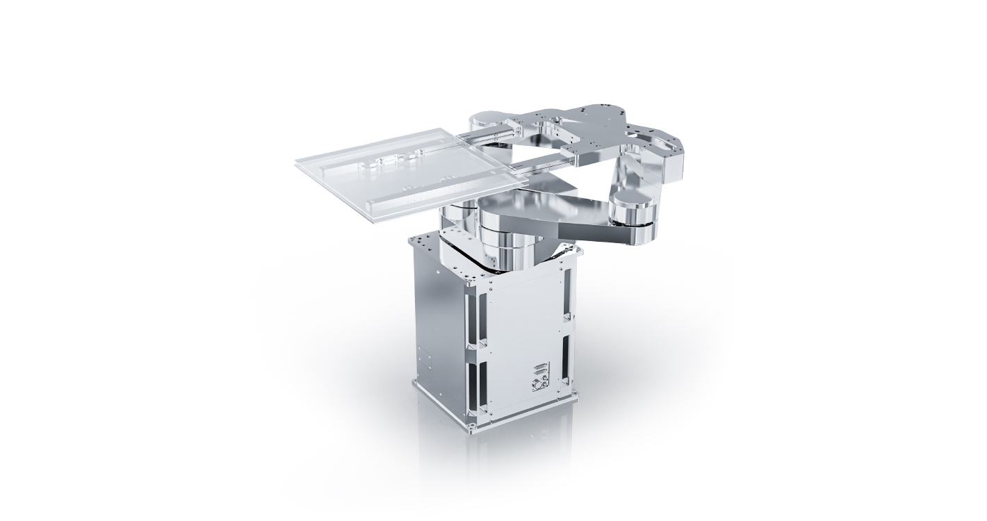
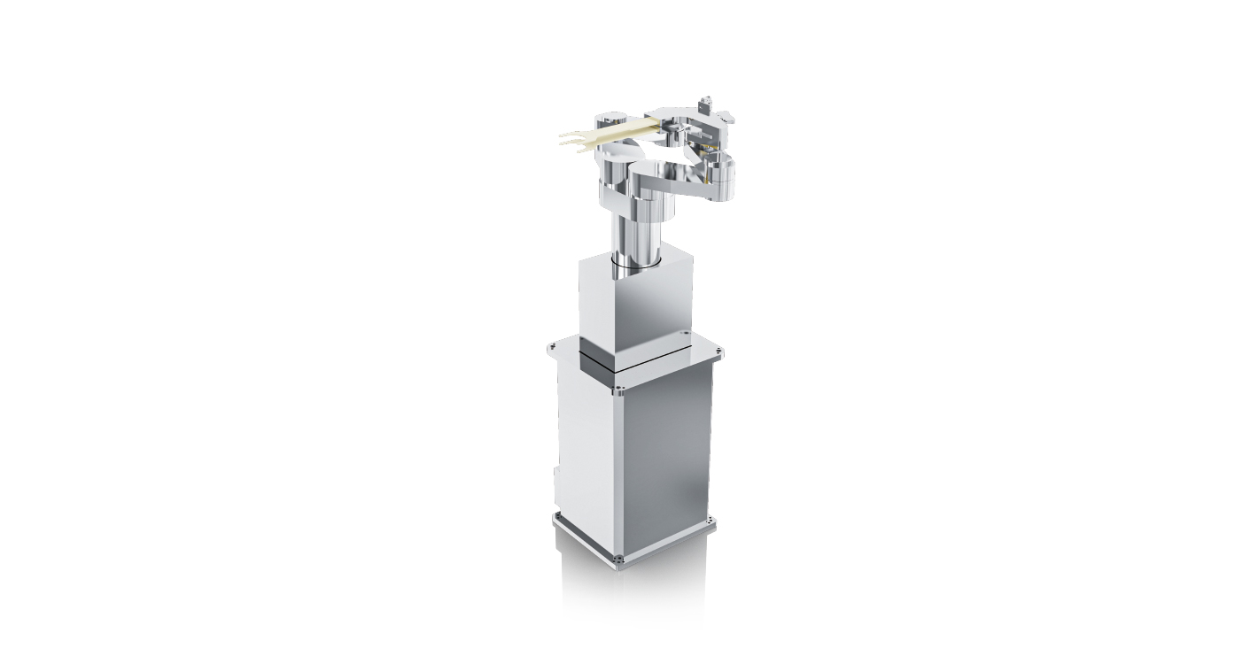
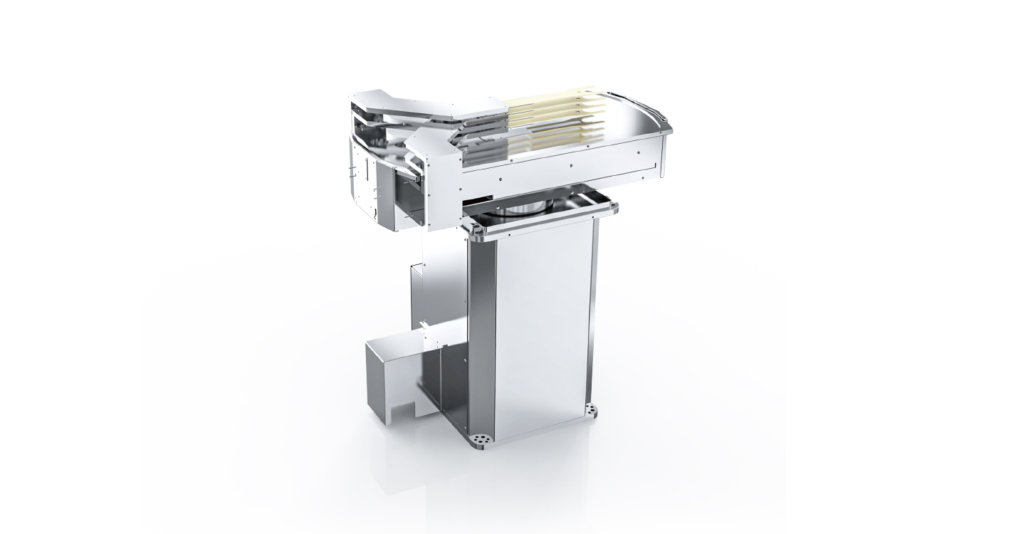
With the trend toward miniaturization and the increasing use of ultra-thin wafers, sorting systems must be capable of handling delicate substrates without causing damage. Modern wafer sorting technology is equipped with sensors and handling mechanisms that can carefully manage ultra-thin wafers and fragile materials, ensuring that no defects occur during the sorting process.
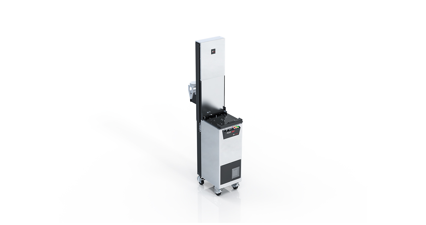
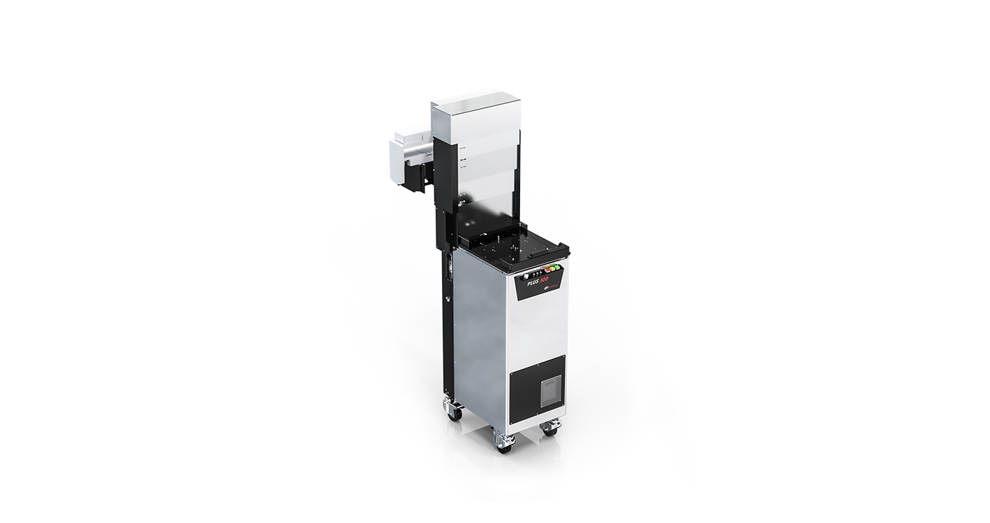
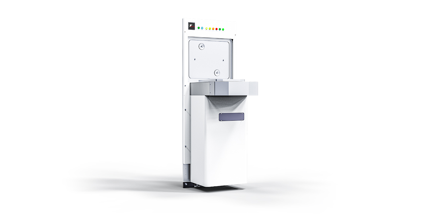
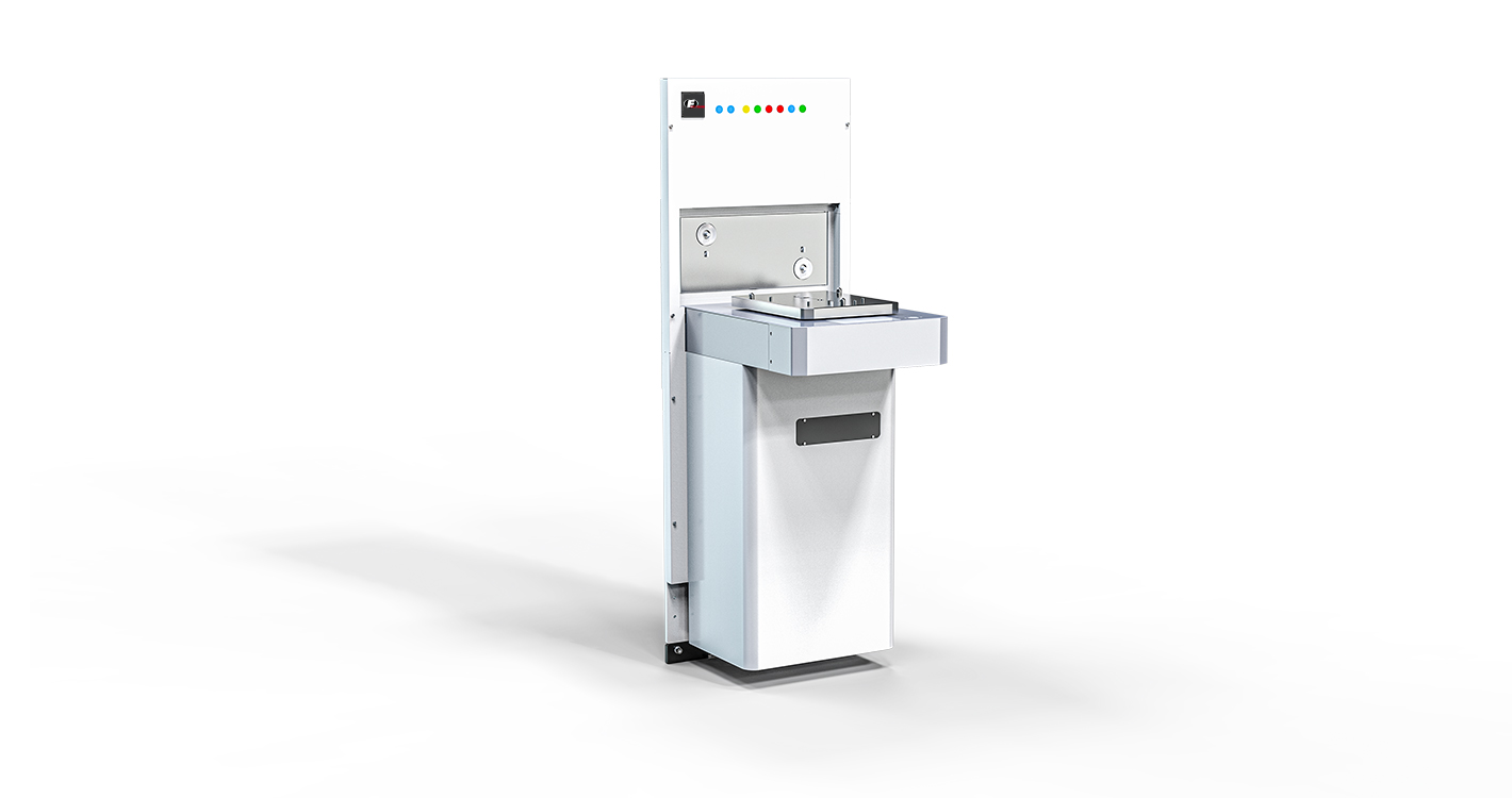
One of the significant advantages of current wafer sorting systems is their ability to handle various wafer types. These systems are designed to accommodate a broad range of wafer sizes, from small 3-inch wafers to larger 12-inch wafers, making them highly versatile for different production environments. Moreover, these systems are also capable of sorting wafers based on different parameters, such as surface flatness, thickness, and defects, allowing for precise categorization of wafers according to production needs.
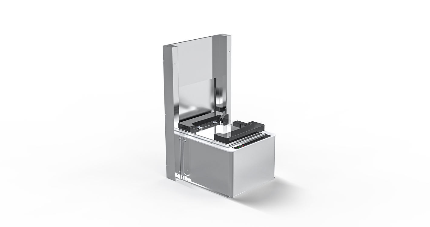
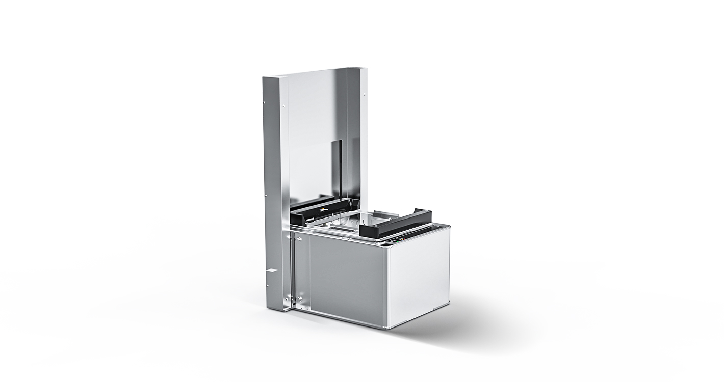
High-precision inspection tools are integral to modern wafer sorting systems. These tools are capable of detecting even the smallest imperfections or irregularities on wafer surfaces. By accurately identifying defects such as scratches, chips, or particles, the sorting system ensures that only high-quality wafers continue down the production line. This reduces waste and increases yield by preventing defective wafers from being processed further.
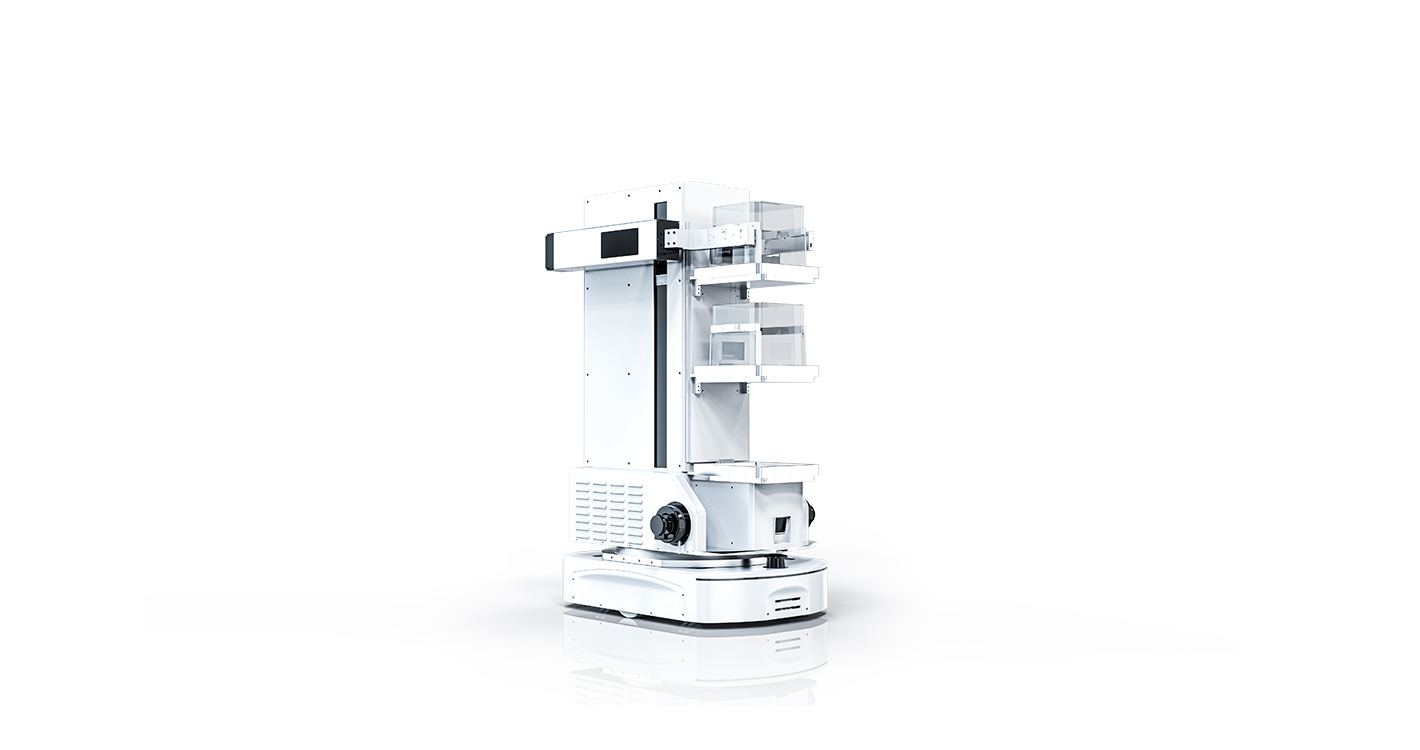
In today’s fast-paced manufacturing environment, it’s essential for new equipment to integrate seamlessly with existing systems. Advanced wafer sorters are designed with flexible interfaces that allow them to be easily integrated into existing production lines. Whether used as standalone units or part of a more extensive automated system, these sorters can be configured to meet the unique requirements of each fab.
By reducing sorting times and improving wafer handling, high-precision wafer sorting systems significantly increase overall throughput. Manufacturers can process more wafers in less time, reducing bottlenecks and improving overall fab efficiency.
With advanced inspection and sorting capabilities, these systems play a crucial role in ensuring that only defect-free wafers are processed further. By identifying and removing faulty wafers early, they contribute to higher product quality and fewer defects in the final semiconductor devices.
As semiconductor devices become more complex, manufacturers increasingly rely on fragile materials that require special handling. Advanced sorting systems are specifically designed to manage such materials, preventing damage during sorting and ensuring that the wafers remain intact throughout the process.
By improving sorting accuracy and reducing waste, advanced wafer sorting systems help fabs save costs in the long term. The ability to quickly detect defects and ensure high-quality output reduces the need for costly rework and ensures higher yields, resulting in overall cost savings.
Wafer sorting is a fundamental process in semiconductor manufacturing, and the latest advancements in sorting technology have brought significant improvements in efficiency, precision, and flexibility. By incorporating high-precision sorting systems into their production lines, fabs can improve throughput, reduce waste, and ensure that only the highest-quality wafers make it to the next phase of production.
Whether dealing with standard wafers or more fragile, complex materials, modern sorting solutions are built to handle the diverse challenges of today’s semiconductor manufacturing environment. With enhanced inspection capabilities, faster sorting speeds, and seamless integration into existing production lines, these systems provide the tools necessary for semiconductor manufacturers to meet the demands of the future.
Interested in learning more about how advanced wafer sorting systems can improve your production line?
Fortrend team of experts is ready to help you find the perfect solution for your specific needs.


Disclaimer: The appearance, specifications, performance descriptions, comparative data, and other information regarding the products displayed on this website are based on internal testing and experiments conducted in FORTREND’s laboratory. This information is for reference purposes only, and the final product may vary.
Copyright © FORTREND. Any commercial promotion of goods or services, whether directly or indirectly to consumers on this website, is considered 'advertising' (excluding product-related information such as packaging, specifications, and after-sales support)
.jpg)
二工位产品中心白底图1420x750.jpg)
二工位产品中心白底图1420x750.jpg)
.jpg)


.jpg)